A Push Pull Converter is dc to dc converter that provides an output voltage that can be either less than or greater than the dc input voltage VS. The push-pull converter give multiple outputs with single input. This can be achieved by changing the winding’s turns ratio of the transformer. Push-pull designs are popularly used in middle to high power applications (150W to 1000W).

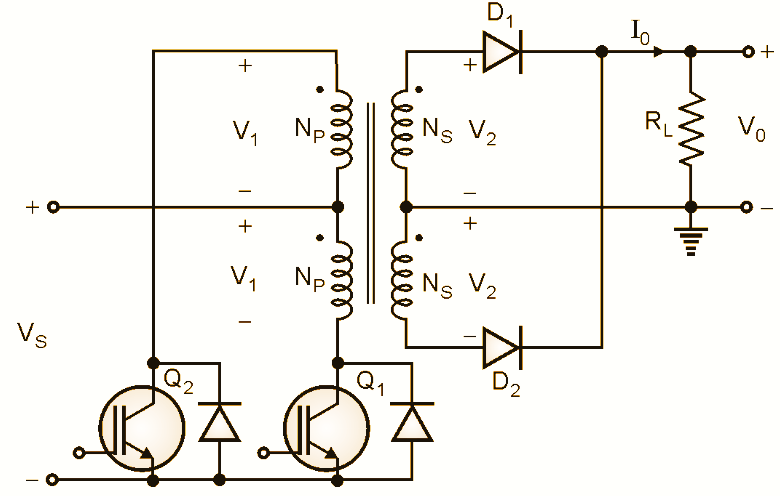
Figure 1: Circuit Diagram of Push Pull Converter.
Circuit diagram & Working of Push Pull Converter
Fig. 1 shows the circuit diagram of a push pull converter. As shown it consists of two transistors, a center tapped transformer and two diodes. Vs is the dc input voltage while Vo is the variable dc output voltage.
1. When Q1 is on :

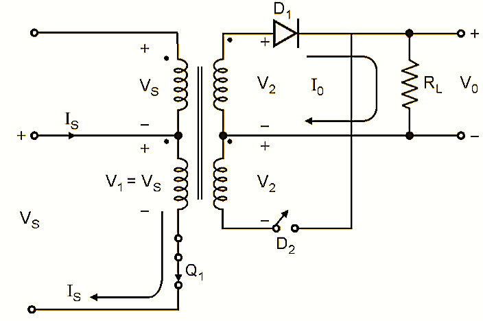
Figure 2: Equivalent Circuit Diagram for mode I (Push Pull Converter).
When transistor Q1 is turned on, the dc input voltage Vs appears across the lower half of the primary winding of the transformer. The equivalent circuit is as shown in Fig. 2. The current through the primary induces the secondary voltage with the polarities shown in Fig. 2. This will forward bias diode D1 and the average output voltage Vo will be positive equal to V2.
\[{{V}_{o}}={{V}_{2}}=({{N}_{s}}/{{N}_{p}}){{V}_{1}}=a{{V}_{1}}=a{{V}_{s}}\]
After half cycle period i.e. t = T/2, transistor Q1 is turned off and Q is turned on. Transistors Q1 and Q2 operate at a 50% duty cycle.
2. When Q2 is on :

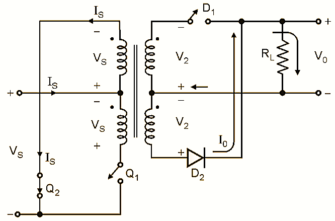
Figure 3: Equivalent Circuit Diagram for mode II (Push Pull Converter).
When transistor Q2 is turned on, the dc input voltage Vs appears across the upper half of the primary winding of the transformer. The equivalent circuit is as shown in Fig. 3. The current through the primary induces the secondary voltage with the polarities shown in Fig. 3. This will forward bias diode D2 and the average output voltage Vo will be positive equal to V2.
\[{{V}_{o}}={{V}_{2}}=({{N}_{s}}/{{N}_{p}}){{V}_{1}}=a{{V}_{1}}=a{{V}_{s}}\]
After the full cycle period i.e. t = T, transistor Q2 is turned off and Q1 is turned on and the cycle of operation repeats itself. Transistors Q1 and Q2 operate at a 50 % duty cycle.
Waveforms of Push Pull Converter
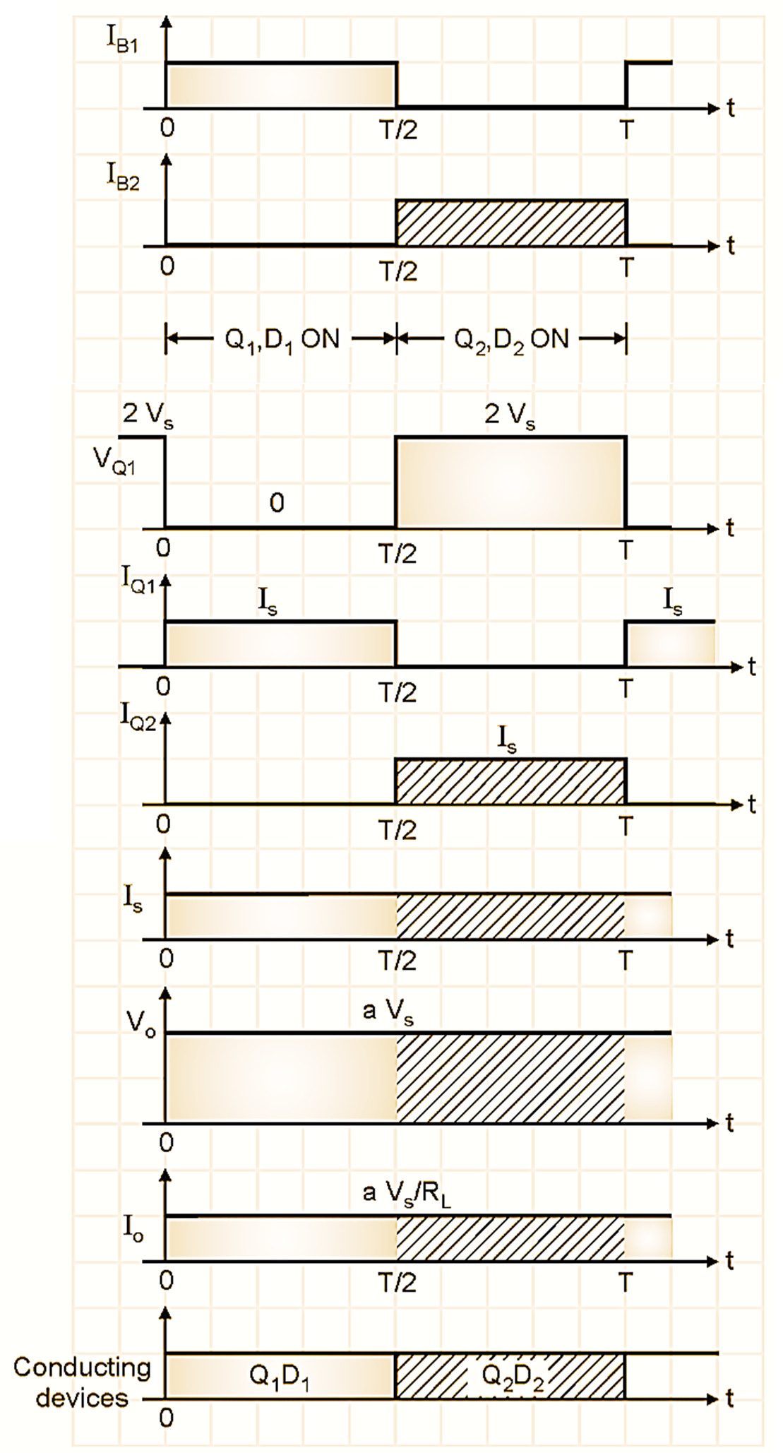
Various voltage and current waveforms for a push-pull converter at 50% duty cycle are as shown in Fig. 4.

Figure 4: Waveforms of Pushk Boost Converter.
Analysis of Push Pull Converter :
1. The average current through each transistor, due to 50% duty cycle is given by :
\[{{I}_{A}}={{I}_{s}}/2\]
2. The peak current through each transistor is equal to the source current is.
\[{{I}_{p}}={{I}_{s}}\]
3. The voltage across a non-conducting transistor is twice the supply voltage. Therefore the push pull configuration is suitable only for low-voltage applications.
Advantages of Push Pull Converter :
The major advantages of a push-pull converter are as follows :
- Low noise operation
- High efficiency
- Multiple outputs
- It provides electrical isolation between input and output.
- Output voltage can be varied above and below the input voltage.
Disadvantages of Push Pull Converter :
The major disadvantages of a push-pull converter are as follows :
- It needs a pair of perfectly matched transistors
- There is a possibility of transformer saturation
- The duty cycle should be kept constant at 50 % to avoid saturation of core.
Applications of Push Pull Converter :
Some of the applications of push-pull converter are as given below :
- Power Supplies
- DC to AC inverter
- DC to DC converter
- Photovoltaic application
- Automotive applications.