In the dc-dc buck converter, the input voltage is constant dc voltage whereas the output voltage is a variable dc voltage and the output voltage is lower than the input voltage. Hence the name dc-dc buck converter.
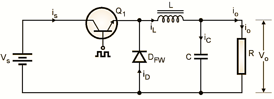
Figure 1: Circuit Diagram of Buck Converter.
Circuit diagram of Buck Converter
Capacitor C1 is the input filter capacitor that may be connected to reduce the ripple in the DC input voltage VS. L and C form an LC filter that connected to reduce the ripple contents in the output of the circuit. DFW is the freewheeling diode. In place of transistor Q1, we can connect any other power switching device like MOSFET or IGBT.
Working of Buck Converter
In the Fig. 1, Q1 is a power transistor which is turned ON and OFF by the rectangular pulses applied at its base. We may connect any other power semiconductor switch in its place. DFW is a freewheeling diode, while L and C form a low pass filter. VS is the unregulated dc power supply.
As we can vary the average output voltage by changing either the duty cycle or frequency. In most application the variation of duty cycle is preferred to variation in frequency. The expression for average output voltage in terms of duty cycle is given by :
\[{{V}_{o}}=D\times {{V}_{S}}\]
The duty cycle “D” can be varied between 0 and 1. Therefore average output voltage Vo will vary between 0 and VS. As average output voltage Vo is less than or equal to VS, this circuit is called as the “buck converter”, or a step down switching regulator. The buck converter is a step down type switching regulator. The operation is divided into two modes.
1. Mode I (When Q1 is on) :
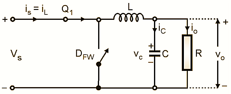
Figure 2: Equivalent Circuit Diagram for mode I (Buck Converter).
When Q1 is turned on the input dc voltage VS gets connected at the input of the LC filter. The output voltage is held constant by the large value capacitor. The current through L increases linearly from I1 to I2. The input current flows through Q1, inductor L, capacitor C, and the load resistance R as shown in Fig. 2. Energy is given to the LC filter and the load during this mode of operation. The diode DFW is reverse biased and remains off.
2. Mode II (When Q1 is OFF) :
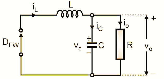
This mode begins at t = t1 when Q1 is turned off. Due to the interruption in current, there is a self induced voltage which appears across the inductance L. This voltage forward biases diode DFW (which is also called as catch diode). The load current starts flowing through the DFW. The inductor current continues to flow through L, C load and the freewheeling diode as shown in Fig. 3. The inductor current reduces linearly from I2 to I1 during this mode of operation. The output voltage can be varied by varying the duty cycle of the power transistor. The output voltage is approximately equal to Vout = DVS
Where,
\[D=\frac{{{T}_{on}}}{{{T}_{on}}+{{T}_{off}}}\]
Waveforms of Buck Converter
The waveforms for a buck converter in the continuous conduction mode are as shown in Fig. 3.
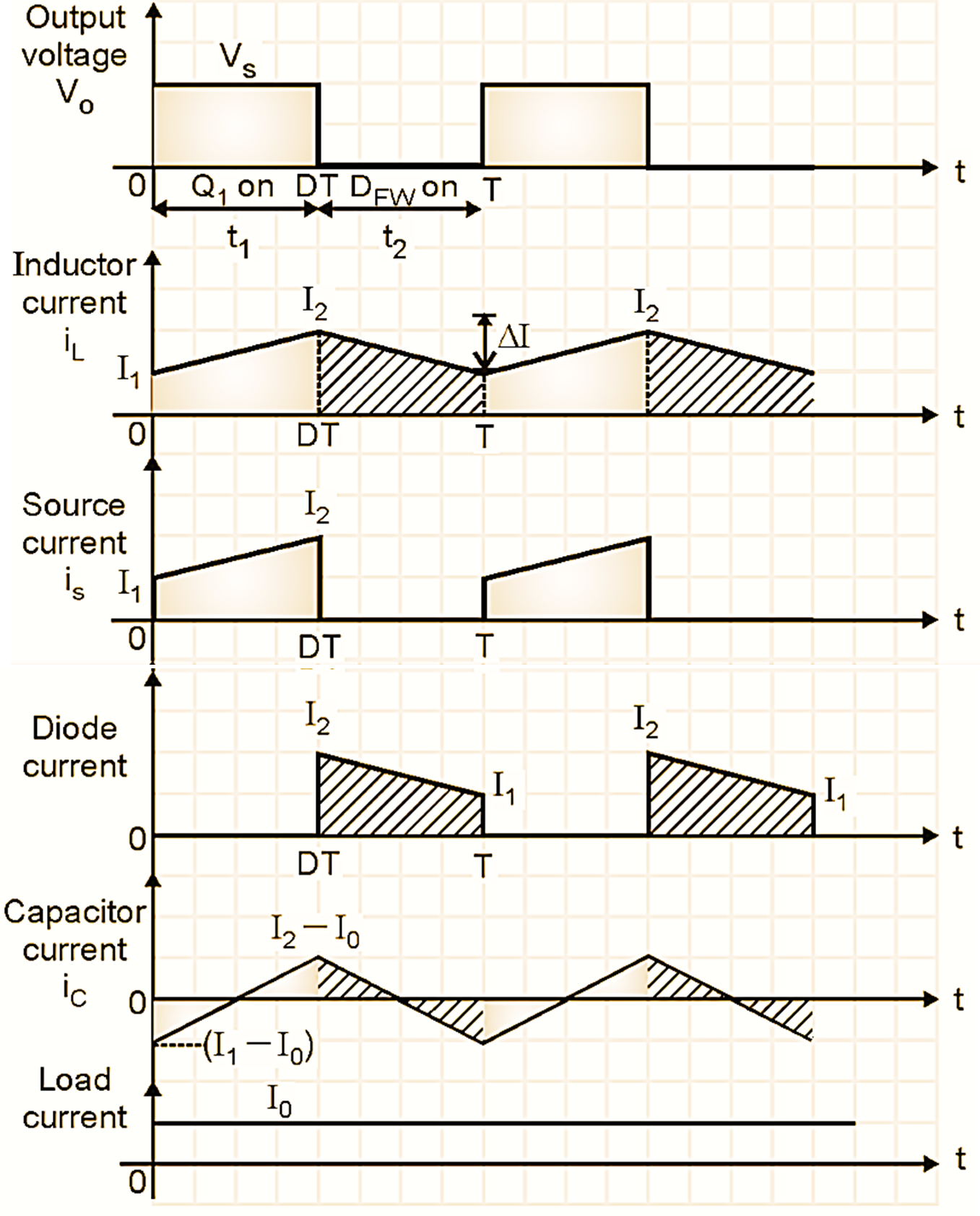
Figure 4: Waveforms of Buck Converter.
Analysis of Buck Converter :
For the analysis of a buck converter we assume the current through filter inductance (iL) is continuous and varies linearly. Also Q1 and DFW are assumed to be ideal devices. Refer the waveforms of Fig. 4, to write the expression for the voltage across L as,
\[{{e}_{L}}=L\frac{d{{i}_{L}}}{dt}\]
The inductor current iL rises linearly from I1 to I2 during time t1.
\[d{{i}_{L}}={{I}_{2}}-{{I}_{1}},dt={{t}_{1}}\]
And the voltage eL during time t1 is VS – Vo as shown in Fig. 2 i.e. equivalent circuit of mode I.
\[{{e}_{L}}={{V}_{S}}-{{V}_{o}}\]
Substituting these value we get, \[{{V}_{S}}-{{V}_{o}}=\frac{L({{I}_{2}}-{{I}_{1}})}{{{t}_{1}}}\]
Let (I2 – I1) = ΔI i.e. the peak to peak ripple current.
\[{{V}_{S}}-{{V}_{o}}=\frac{L\Delta I}{{{t}_{1}}}\]
\[{{t}_{1}}=\frac{L\Delta I}{{{V}_{S}}-{{V}_{o}}}….(1)\]
Now consider mode II of operation. Here iL changes linearly from I2 to I1 in time t2. As shown in Fig. 3 the voltage eL during this mode is equal to (-Vo).
\[{{e}_{L}}=\frac{Ld{{i}_{L}}}{dt}\]
\[\text{But, }{{i}_{L}}={{I}_{2}}-{{I}_{1}}\text{ and dt = }{{\text{t}}_{2}}\]
\[-{{V}_{o}}=\frac{-L({{I}_{2}}-{{I}_{1}})}{{{t}_{2}}}=\frac{-L\Delta I}{{{t}_{2}}}\]
\[{{t}_{2}}=\frac{L\Delta I}{{{V}_{o}}}….(2)\]
Equating the values of ΔI in Equations (1) and (2) we get,
\[\Delta I=\frac{{{t}_{1}}({{V}_{S}}-{{V}_{o}})}{L}=\frac{{{V}_{o}}{{t}_{2}}}{L}….(3)\]
But t1 = DT and t2 = (1 – D) T. Substituting these values into Equation (3) we get the average output voltage of a buck converter as,
\[DT({{V}_{S}}-{{V}_{o}})={{V}_{o}}(1-D)T\]
\[{{V}_{S}}DT-{{V}_{o}}DT={{V}_{o}}T-{{V}_{o}}DT\]
\[{{V}_{S}}DT={{V}_{o}}T\]
\[{{V}_{o}}=D{{V}_{S}}\]
Now assume that the buck converter circuit is lossless.
\[\text{Input power = Output power}\]
\[{{V}_{S}}{{I}_{S}}={{V}_{o}}{{I}_{o}}=D{{V}_{S}}{{I}_{o}}….(4)\]
From equation (4) we get the average source current as,
\[{{I}_{S}}=D{{I}_{o}}\]
Switching period T :
The switching period T is given by,
\[T={{t}_{1}}+{{t}_{2}}….(5)\]
Substituting Equations (1) and (2) into Equation (5) we get,
\[T=\frac{L\Delta I}{{{V}_{S}}-{{V}_{o}}}+\frac{L\Delta I}{{{V}_{o}}}\]
\[T=\frac{L\Delta I({{V}_{o}}+{{V}_{S}}-{{V}_{o}})}{{{V}_{o}}({{V}_{S}}-{{V}_{o}})}\]
\[T=\frac{L\Delta I\text{ }{{V}_{S}}}{{{V}_{o}}({{V}_{S}}-{{V}_{o}})}….(6)\]
Peak to peak ripple current ΔI :
From Equation (6) we get,
\[\Delta I=\frac{T{{V}_{o}}({{V}_{S}}-{{V}_{o}})}{L{{V}_{S}}}\]
But T = 1/f and Vo = DVS.
\[\Delta I=\frac{D{{V}_{S}}({{V}_{S}}-D{{V}_{S}})}{fL{{V}_{S}}}\]
\[\Delta I=\frac{D{{V}_{S}}(1-D)}{fL}\]
Advantages of Buck Converter
The advantages of buck converter are as follows .
- It needs only one transistor.
- It is a simple circuit.
- The circuit efficiency is high (higher than 90%).
- The di/dt of the load current is limited by inductor L.
Disadvantages of Buck Converter
The disadvantages of buck converter are as follows :
- Input current is discontinuous and a smoothing input filter is generally required.
- It can produce an output voltage of only one polarity. Polarity reversal is not possible.
- The output current is unidirectional.
- It needs a separate protection circuit against a possible short circuit, across the diode path.