A buck-boost converter provides an output voltage that can be either less than or greater than the dc input voltage VS. Hence the name “buck boost”. The output voltage polarity is opposite to that of the input voltage. It is a combination of buck and boost converters.
Circuit diagram & Working of Buck Boost Converter
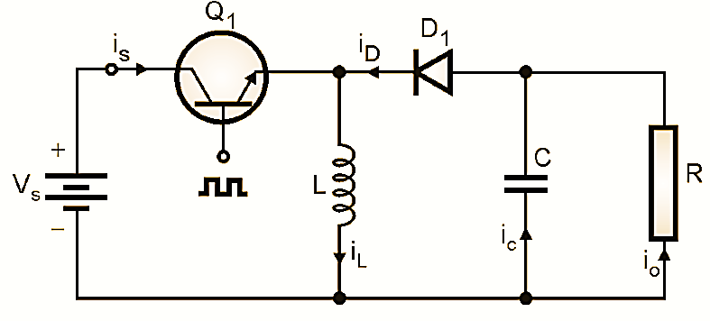
The circuit diagram for the buck boost converter is as shown in Fig. 1. The buck boost switching converter is a non-isolated type converter and it is also known as inverting converter. The buck-boost converter is a type of flyback converter whose operation is very similar to a boost converter. A power BJT is used as a switching device in Fig. 1. But it is possible to use either a MOSFET or an IGBT in place of the power BJT. The operation can be divided into two modes.
1. Mode I (Q1 ON):
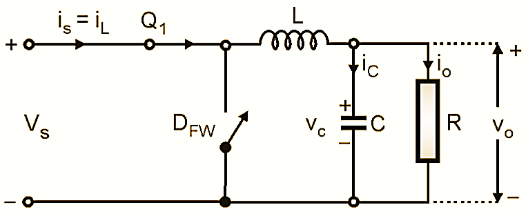
When Q1 is turned on at t = 0, the supply voltage VS gets connected across the inductance L and Diode D1 is reverse biased. The inductance current starts increasing linearly from I1 to I2. The inductance will store energy during this mode of operation. Fig. 2 shows the equivalent circuit for this mode.
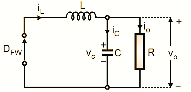
2. Mode II (Q1 off D1 on):
As soon as the transistor Q1 is turned off at t = t1, the current through L is interrupted abruptly. A negative voltage is induced into L which will forward bias diode D1. The load current starts flowing through D1, C and L as shown in Fig. 3. Note that this current is negative. The capacitor charges with its lower plate positive with respect to its upper plate. During this mode the energy stored in L is delivered to the load and the inductor current decreases from I2 to I1 linearly until transistor Q1 is turned on again. This mode comes to an end when Q is turned on again in the next cycle of operation. Fig. 3 shows the equivalent circuit for this mode.
Waveforms of Buck Boost Converter
The waveforms for a buck boost converter in the steady state for the continuous conduction mode are as shown in Fig. 4.
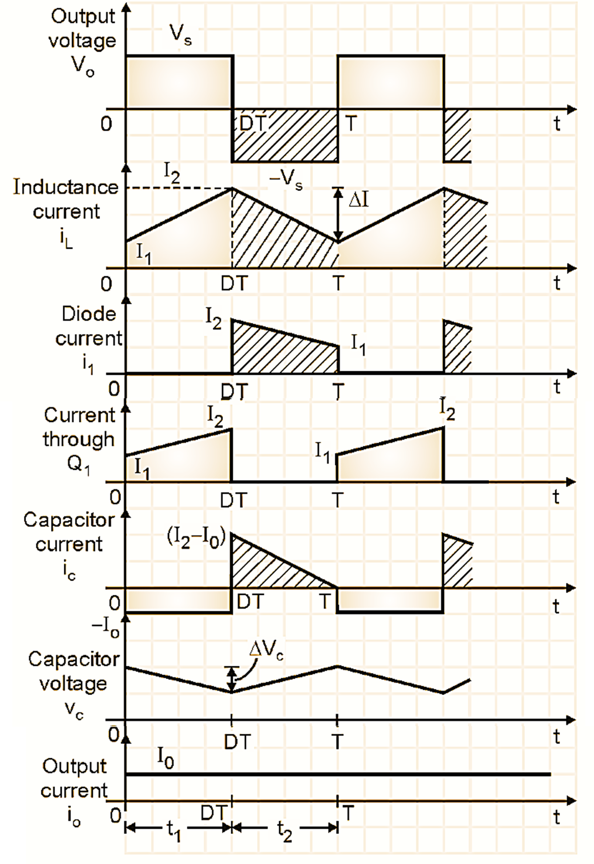
Figure 4: Waveforms of Buck Boost Converter.
Analysis of Buck Boost Converter :
Refer Fig. 4. The inductor current increases from I1 to I2 in time t.
\[{{e}_{L}}=\frac{Ld{{i}_{L}}}{dt}….(1)\]
But in mode I, eL = VS, d iL = I2 – I1 = ΔI and dt = t1.
\[{{V}_{S}}=\frac{L({{I}_{2}}-{{I}_{1}})}{{{t}_{1}}}=\frac{L\Delta I}{{{t}_{1}}}\]
\[\text{OR }{{t}_{1}}=\frac{L\Delta I}{{{V}_{S}}}\]
In mode II, the inductor current falls linearly from I2 to I1 in time t2 and eL = -Vo. Substituting all these values into Equation (1) we get,
\[{{V}_{o}}=\frac{-L\Delta I}{{{t}_{2}}}\]
Therefore,
\[{{t}_{2}}=\frac{-L\Delta I}{{{V}_{o}}}\]
Note that ΔI = (I2 – I1) is the peak to peak ripple in the inductor current. From above Equations we get,
\[\Delta I=\frac{{{V}_{S}}{{t}_{1}}}{L}=\frac{-{{V}_{o}}{{t}_{2}}}{L}\]
But t1 = On time = DT and t2 = Off time = (1 – D)T.
\[{{V}_{S}}(DT)=-{{V}_{o}}(1-D)T\]
Hence the average output voltage of the buck boost converter is,
\[{{V}_{o}}=\frac{-D{{V}_{S}}}{(1-D)}….(2)\]
\[(1-D)=\frac{-D{{V}_{S}}}{{{V}_{S}}}….(3)\]
Substitute t1 = DT and t2 = (1 – D) T in Equation (3) we get,
\[(1-D)=\frac{-{{V}_{S}}}{{{V}_{o}}-{{V}_{S}}}….(4)\]
Now substitute t2 = (1 – D) T and the value of (1 – D) from Equation (4) into Equation (2) to get,
\[{{t}_{1}}=\frac{{{V}_{o}}}{({{V}_{o}}-{{V}_{S}})f}\]
Assume that the buck-boost converter is a lossless circuit.
\[{{V}_{S}}{{I}_{s}}=-{{V}_{o}}{{I}_{o}}\]
\[\text{But }{{V}_{o}}=\frac{-D{{V}_{S}}}{(1-D)}\]
\[{{V}_{S}}{{I}_{s}}=\frac{D{{V}_{S}}}{(1-D)}.{{I}_{o}}\]
Hence the average input current Is is given by,
\[{{I}_{s}}=\frac{D{{I}_{o}}}{1-D}\]
The switching time T is given by,
\[T={{t}_{1}}+{{t}_{2}}\]
Substituting t1 and t2 from above Equations we get,
\[T=\frac{L\Delta I}{{{V}_{S}}}-\frac{L\Delta I}{{{V}_{o}}}\]
\[T=\frac{1}{f}=\frac{L\Delta I({{V}_{o}}-{{V}_{S}})}{{{V}_{o}}{{V}_{S}}}\]
Hence the peak to peak ripple current is given by,
\[\Delta I=\frac{{{V}_{o}}{{V}_{S}}}{fL({{V}_{o}}-{{V}_{S}})}\]
Substitute \({{V}_{o}}=\frac{-D{{V}_{S}}}{(1-D)}\) to get,
\[\Delta I=\frac{-DV_{s}^{2}}{(1-D)}\times \frac{1}{fL\left[ \frac{-D{{V}_{S}}}{1-D}-{{V}_{S}} \right]}\]
\[=\frac{-DV_{s}^{2}}{(1-D)fL}.\frac{(1-D)}{-D{{V}_{S}}-(1-D){{V}_{S}}}\]
\[=\frac{-DV_{s}^{2}}{(1-D)fL}\times \frac{(1-D)}{-{{V}_{S}}(D-1-D)}\]
\[\Delta I=\frac{D{{V}_{S}}}{fL}\]
Expression for the voltage ripple :
When Q1 is conducting during mode I, the filter capacitor C supplies the load current for t1.
The average discharging current of capacitor C is,
\[{{I}_{c}}={{I}_{o}}\]
Hence the peak to peak ripple voltage of the capacitor is given by,
\[\Delta {{V}_{c}}=\frac{1}{C}\int\limits_{0}^{{{t}_{1}}}{{{I}_{c}}dt}\]
\[=\frac{1}{C}\int\limits_{0}^{{{t}_{1}}}{{{I}_{o}}dt}\]
\[{{V}_{c}}=\frac{{{I}_{o}}{{t}_{1}}}{C}\]
Substituting t1 we get,
\[\Delta {{V}_{c}}=\frac{{{I}_{o}}{{V}_{o}}}{C({{V}_{o}}-{{V}_{S}})f}\]
Substitute \(\Delta {{V}_{c}}=\frac{D{{V}_{d}}}{(1-D)}\) and simplify to get,
\[\Delta {{V}_{c}}=\frac{D{{I}_{o}}}{fC}\]
Advantages of Buck Boost Converter :
Some of the important advantages of buck-boost converter are as follows :
- This circuit produces a negative output voltage without transformer.
- Its efficiency is high.
- The rate of change of fault current (di/dt) is limited to a safe value by the inductor L.
- It is easy to implement the short circuit protection.
Disadvantages of Buck Boost Converter :
Some of the important disadvantages of buck boost converter are as follows :
- Input current is discontinuous.
- A high peak current flows through the transistor.