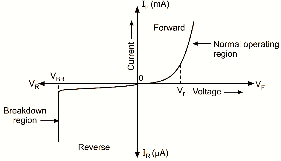
Figure 1: V-I Characteristics of a PN Junction Diode.
VI Characteristics of pn junction diode, is a graph between the voltage applied across the terminals of a device and the current that flows through it. Fig. 1 shows the V-I characteristics of a typical PN junction diode with respect to breakdown voltage (VBR). The complete V-I characteristics is divided into two parts, namely forward characteristic and reverse characteristic.
Forward characteristics :
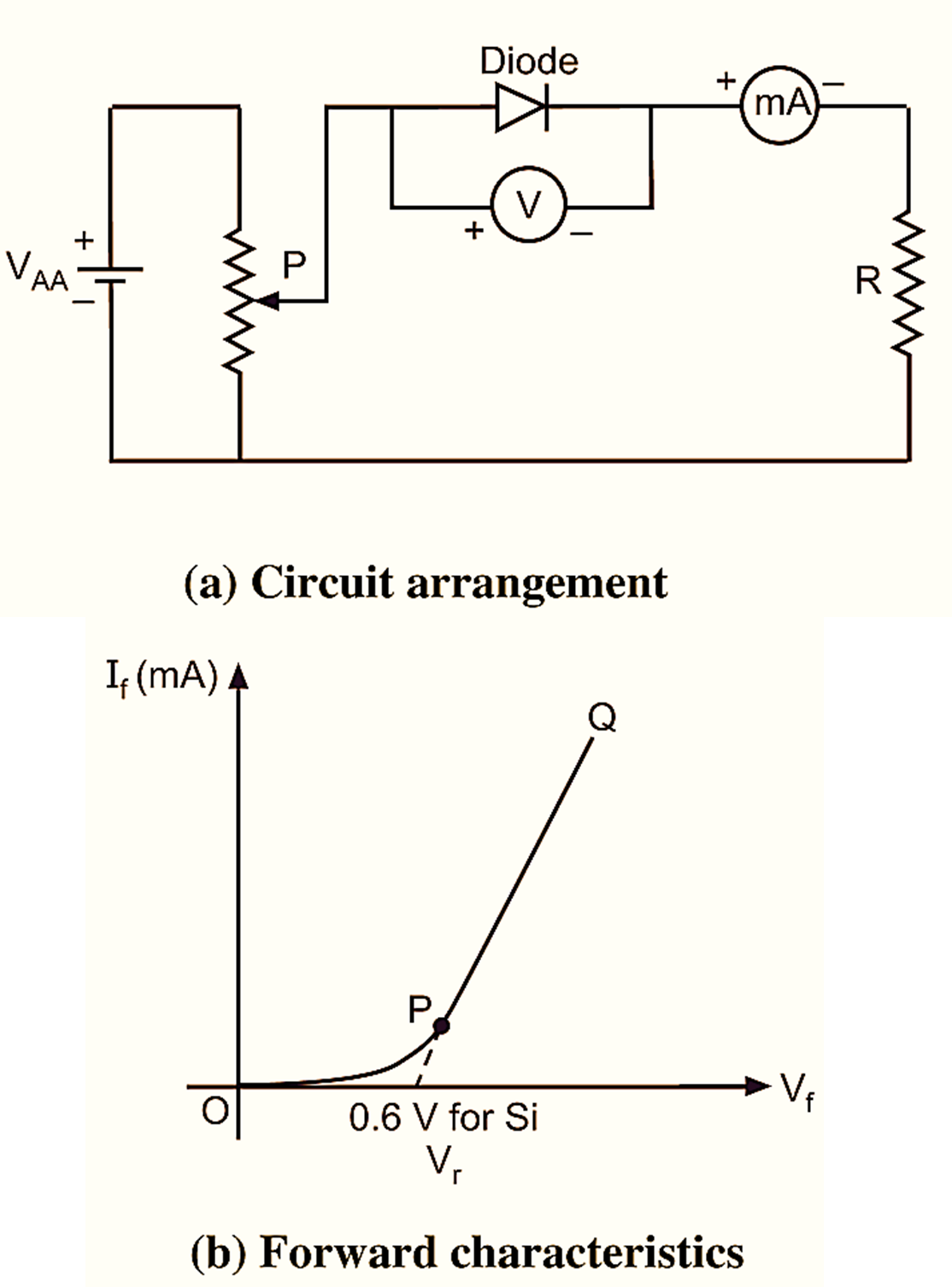
Figure 2.
Fig. 2 (a) shows the circuit arrangement for obtaining forward characteristic of a diode. In this circuit, the diode is connected to a d.c. voltage (VAA) through the potentiometer (P) and a resistance (R). The potentiometer helps in varying the voltage applied across the diode. The resistance (R) is included in the circuit, so as to limit the current through the diode. A voltmeter is connected across the diode to measure the voltage and milliammeter to measure the current in the circuit. The positive terminal of the voltage source is connected to the anode and the negative terminal to the cathode, hence the diode is worked in forward-biased condition. Increase the voltage and record the corresponding values of diode current. The graph between applied voltage and current is plotted as shown in Fig. 2 (b).
Forward characteristics show that no current flow till the point P is reached. It is due to the fact that, applied voltage is less than the junction voltage i.e. 0.7 V for Silicon and 0.3 V for Germanium. As the voltage is increased above point P, the diode current increases rapidly. The voltage at which the diode starts conducting is called a knee voltage, cut-in voltage or threshold voltage. The knee voltage is denoted by VR or Vγ. Its value is 0.6 V for Si and 0.2 V for Ge.
Reverse characteristics :
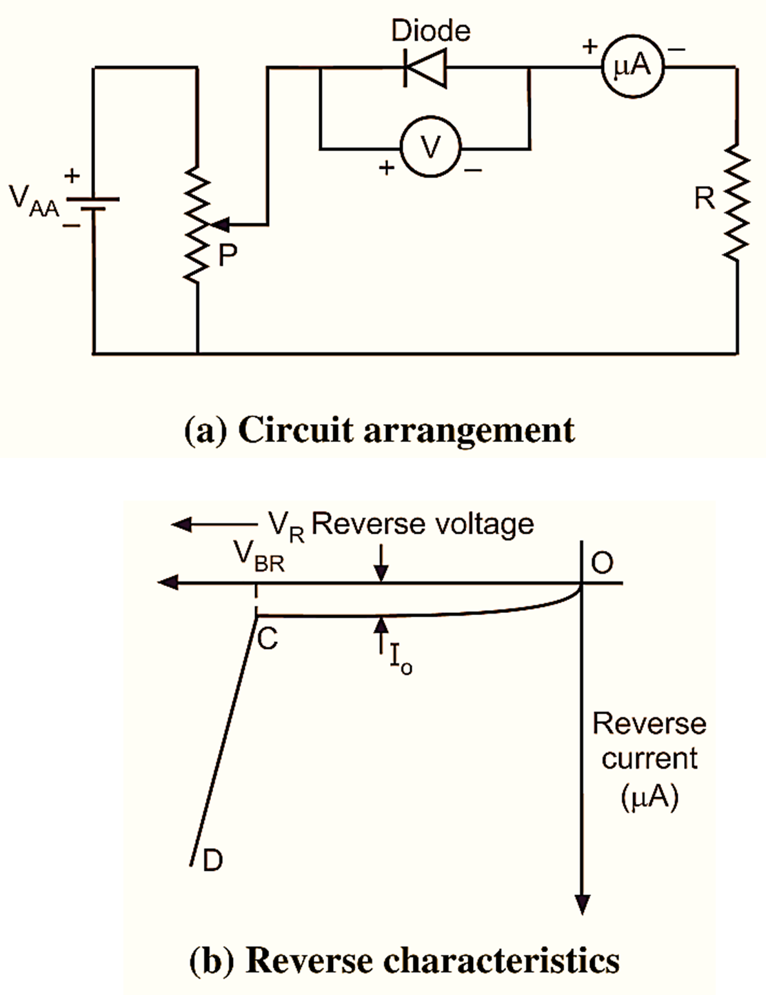
The circuit arrangement for obtaining reverse characteristics of a diode is shown in Fig. 3 (a). In the circuit a diode is connected in reverse biased condition i.e. cathode is connected to the positive terminal of voltage source and anode to the negative terminal. The applied reverse voltage is gradually increased above zero and the values of diode current are measured. The graph plotted between reverse voltage and current is shown in Fig. 3 (b). The curve OCD is called reverse characteristics of a diode. The reverse characteristics indicate that when applied reverse voltage is less than breakdown voltage (VBR), the diode current is small and remains constant. This current is called as reverse saturation current (Io).
When reverse voltage is increased to a large value, the diode reverse current increases as rapidly as shown by curve CD in Fig. 3. The applied reverse voltage at which large current flows through the diode is known as breakdown (VBR) voltage of a diode.