An N-channel JFET is fabricated (or constructed) on N-type semiconductor bar that is as shown in figure (1). The left end of the N-type semiconductor bar is known as source and the right end is known as drain.
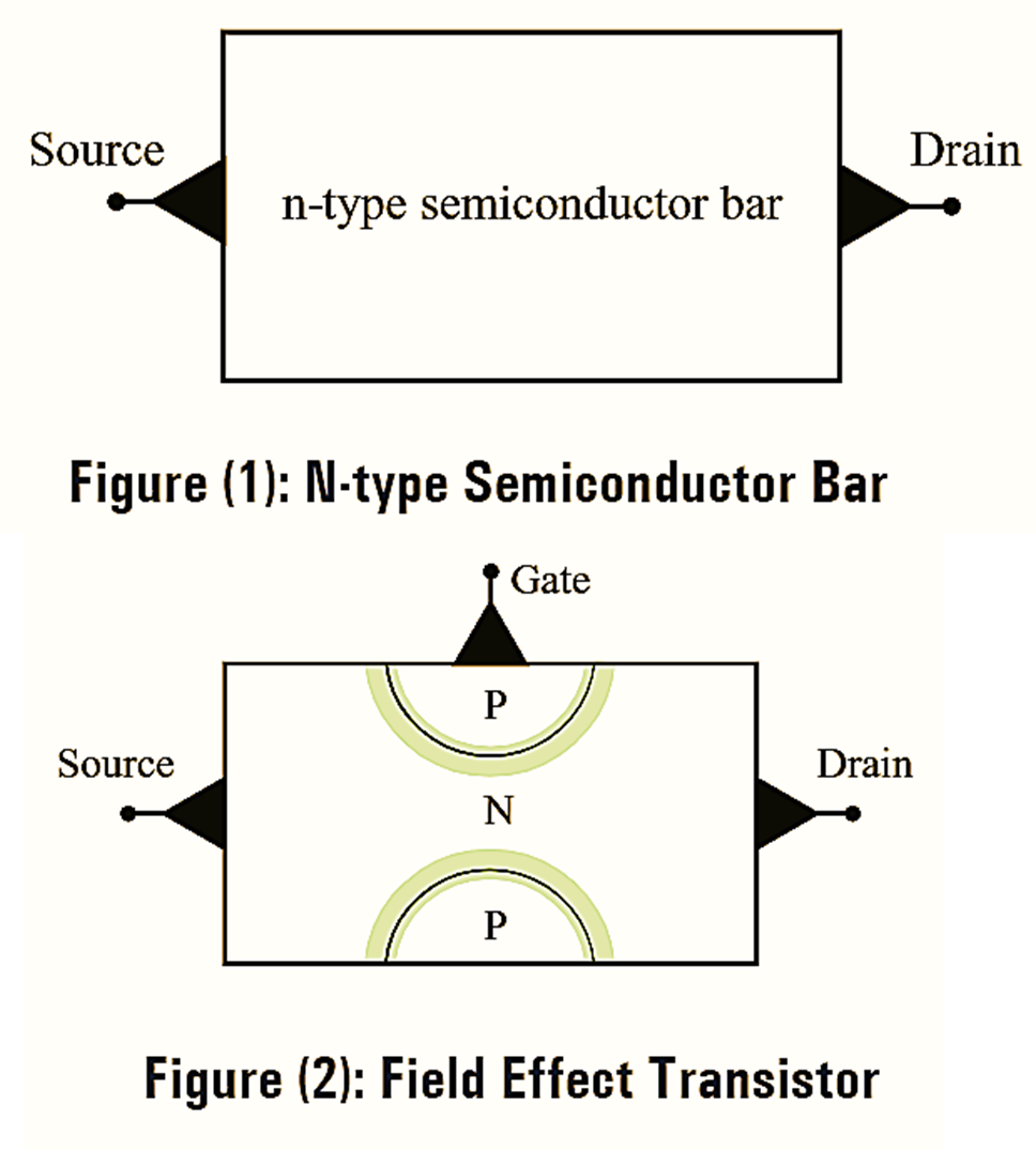
Construction of N-channel JFET
To design a N-channel JFET, the N-type bar is heavily doped with two P-type regions at both the ends as shown in figure (2). The P-type regions are introduced into N-type bar using diffusion process. Both the P-type regions are connected internally and a single wire is taken out in the form of a terminal called a gate. Diffusion of P-type regions into N-type region creates two PN-junctions (shaded region) as shown in figure (2).
Working of N-channel JFET
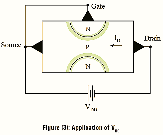
Initially, with VGS = 0 V and application of a voltage VDD across the drain and source terminals as shown in figure (3), causes a current ID to flow from drain to source.
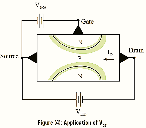
The current ID flowing through the N-channel can be controlled by applying a negative voltage to the gate and source terminals as shown in figure (4). The negative VGG reverse biases the two p-n junctions and increases the width of depletion regions. The depletion region extends (or spreads) more into the N-channel because it is doped lightly compared top-regions. In other words, to make the depletion region extend more into the N-channel, the two p-regions are doped very heavily. The extension of depletion region decreases the width of the channel as shown in figure (4). This in tum decreases the current ID flowing through the channel. Since the current ID flowing through the channel is controlled by the voltage VGS JFET is known as voltage controlled device.
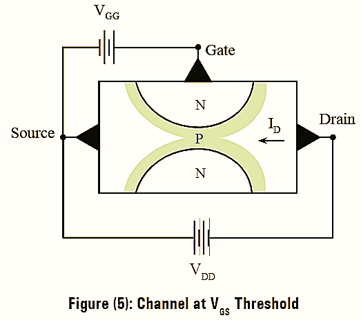
Continuous increase in the negative voltage VGS can cause the depletion region to extend more and more into the channel. Finally, the entire channel gets occupied by the depletion region and depleted of charge carriers (electrons) as shown in figure. The value of VGS at which the entire channel gets occupied by the depletion-region is known as ‘threshold voltage’ of the device ‘Vt‘. For JFETs the threshold voltage is called the “pinch-off voltage” and is denoted by ‘VP‘.