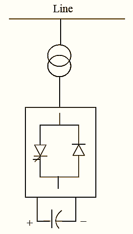
Figure 1: Voltage Source Converter.
Symbolic representation of a voltage sourced convener is as shown in figure 1. The symbol has a box with a gate tum-off device paralleled by a reverse diode, and a D.C capacitor as its voltage source.
In a voltage source converter, devices undergo sequential switching to present unidirectional D.C voltage of a D.C capacitor, as A.C voltage to the A.C side. The A.C output voltage can be varied in magnitude and also in any phase relationship to the A.C system voltage, using suitable converter topology. The power reversal here involves only the reversals of current but not the voltage. In case the storage capacity of the D.C capacitor reduces and if the D.C capacitor has no other source of power, the converter can no more impart or consume the real power for more than a cycle. A converter imparts or absorbs the reactive power alone, as long as the A.C voltage and A.C current (leading or lagging) are at 90º phase angle, where the A.C current is taken as reference.
Basic Operating Principle of a Voltage Source Converter
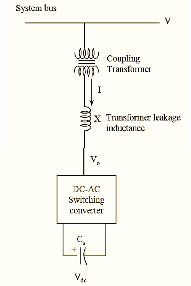
Figure 2: Voltage Source Converter working principle.
The basic operating principle of a voltage source converter generating reactive power is comparable to that of a conventional rotating synchronous machine (see Figure 2). Single line diagram for a basic voltage source convener scheme for reactive power generation is as shown in figure. The convener gives a set of controllable three phase output voltage with system frequency by the charged capacitor CS when a D.C input voltage is given. Each output voltage is in phase with and coupled to the respective A.C system voltage through a small tie reactance. The tie reactance is of the order 0.1 to 0.15 p.u and it is provided by the per phase leakage inductance of the coupling transformer. The reactive power exchange between the converter and the A.C system is controlled by changing the amplitude of output voltage produced. This means that when the output voltage is increased than that of the A.C system voltage, current flows via the tie reactance from the converter to the A.C system. Thus reactive (capacitive) power for the A.C system is generated by the convener. Now if the output voltage is decreased then the reactive current flows to the converter from the A.C system. Thus reactive (inductive) power is absorbed by the converter. In case if the output voltage and the A.C system voltage are equal in amplitude, the reactive power exchange is zero.
Circuit Diagram of a Voltage Source Converter
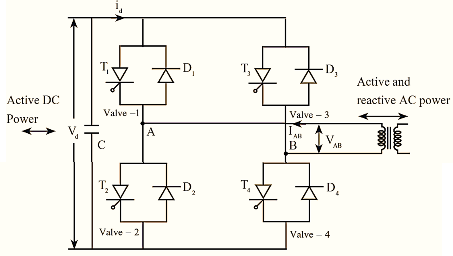
Figure 3: Circuit Diagram of a Voltage Source Converter
The circuit diagram of single-phase full wave bridge converter is shown in figure (3).
Working of a Voltage Source Converter
Voltage source converter generates A.C voltage from D.C voltage. A single phase full wave bridge converter consists of 4 valves, namely valve-1, valve-2, valve-3 and valve-4 and each valve consists of a turn-off device T, and diode D, connected in series with each other. On the D.C side, as the voltage is unipolar, it is supported by a capacitor. The capacitor is used to handle the current that accompanies the switching sequence of the converter valve and shifts in phase angle of the switching valves without change in D.C voltage and two ac connection points A and B.
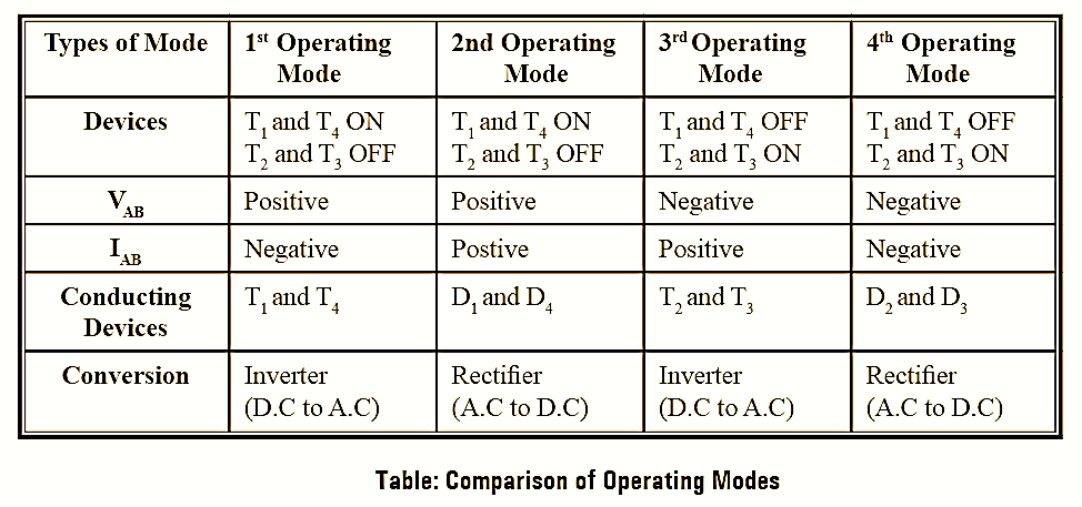
Conversion of AC voltage to D.C voltage is possible by changing the turn-ON and turn-OFF sequence of valves. In one cycle the single phase full wave bridge operates in four different operating modes as given below,
- T1 and T4 ON, T2 and T3 OFF (Inverter)
- T1 and T4 ON, T2 and T3 OFF (Rectifier)
- T1 and T4 OFF, T2 and T3 ON (Inverter)
- T1 and T4 OFF, T2 and T3 ON (Rectifier)
When the turn-off devices T1 and T4 are turned ON, voltage becomes positive i.e., +Vd for one half cycle and with T2 and T3 turned ON, VAB becomes negative. The interaction of the converter generated A.C voltage with the A.C system voltage and impedance results in A.C current, which is generally a sinusoidal wave form.
From the 1st operating mode time ta to tb with the turn-off devices T1 and T4 ON and T2 and T3 off, VAB is positive and current iAB is negative. Here power flow is from D.C to A.C. Hence inversion action takes place. In 2nd operating mode time tb to tc, the current iab is positive and flows through diodes D1 and with power flow A.C to D.C. Hence, it acts as a rectifier. Similarly 3rd and 4th operating modes are conducted. The operations of all the modes are shown below in comparison table.
The output waveforms of single phase converter is shown in figure (4).
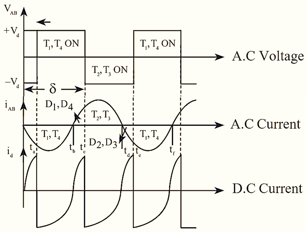
Figure 4.
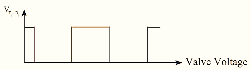
Figure 5.
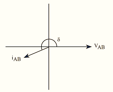
Figure 6.
Figure 4 gives the output waveforms of voltage and current as per the given table. Figure 5 is the voltage across the valve 1 i.e., VT1-D1. It is also known as lost waveform. Figure 6 shows the power flow from A.C to D.C with a power factor lagging. It gives the relationship between A.C voltage and current phasors.
Disadvantages of a Voltage Source Converter
The following are the disadvantages of voltage-source converters,
- The output current limitation is low and it cannot control the capability of the semi-conduction device system faults.
- In voltage-source converter, it is very difficult to protect converter against internal faults.
- They have high-short circuit current and the transformer connections are complex compared with CSC.
- Rapid increase in rise of capacitor discharge current results in the damage of valves.