A Silicon Controlled Rectifier (SCR) is a four-layer, three-junction semiconductor device used as a switch and rectifier in power control applications. It belongs to the family of thyristors and operates as a controllable switch. SCRs are widely used in industrial electronics, motor control, light dimming, and voltage regulation.
A silicon-controlled rectifier is a four-layer PNPN device with a gate control terminal. Basically, it is a semiconductor device made of silicon material.
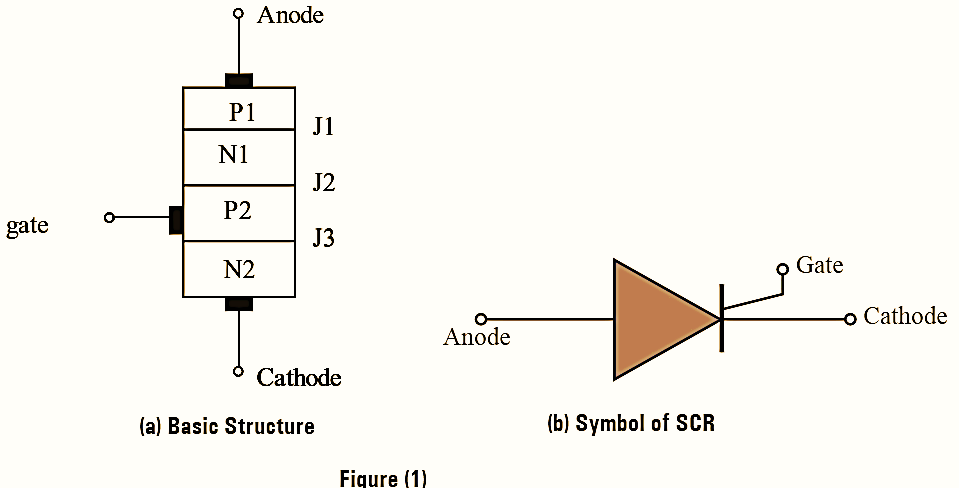
Construction of Silicon Controlled Rectifier (SCR)
It consists of four layers (i.e., P1, N1, P2 and N2), three terminals A(Anode), C(Cathode) and G(Gate) and three junctions J1 J2 and J3. The SCR consists of see figure 1(a):
- Four alternate layers of P-type and N-type materials, forming three PN junctions (J1, J2, J3).
- Three terminals:
- Anode (A): Connected to the outermost P-layer (i.e. P1).
- Cathode (K): Connected to the outermost N-layer (i.e. N2).
- Gate (G): Connected to the P-layer (i.e. P2) near the cathode. Used to trigger the SCR.
- Three PN junctions (J1, J2, J3): The middle junction (J2) is reverse-biased during normal operation until triggered.
Modes of Operation of Silicon Controlled Rectifier (SCR)
SCR operates in three modes:
- Forward Blocking Mode (Off-state): When the anode is positive concerning the cathode, J1 and J3 are forward-biased, but J2 is reverse-biased, preventing current flow.
- Forward Conduction Mode (On-state): A small current applied to the gate terminal (gate triggering) reduces the reverse bias of J2, allowing the SCR to conduct. The device latches into the “on” state, and current flows freely from anode to cathode. Removing the gate signal does not turn off the SCR; it remains on until the anode current drops below a specific holding current.
- Reverse Blocking Mode: When the cathode is positive concerning the anode, J1 and J3 are reverse-biased, and the SCR blocks the current.
Working of Silicon Controlled Rectifier (SCR)
The basic structure of SCR is illustrated in figure 2.
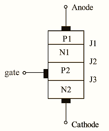
Figure 2: Silicon Controlled Rectifier (SCR) Structure.
The anode and cathode terminals are connected to the main power circuit whereas, the gate terminal is connected to the control circuit. Whenever the P-layer (i.e. P1) near the anode is made more positive, when compared to N-layer (i.e. N2) near the cathode, junctions J1 and J3 are forward biased and the middle junction J2 is reverse biased, and it acts as a capacitor in this mode. Due to the depletion layer formed at this junction, no current flows through the device, but due to the drift carriers, a small amount of leakage current flows through the circuit.
As the leakage current is negligibly small, the device operates in OFF state and blocks forward voltage. This state is known as forward blocking state. Whenever the N-layer (i.e. N2) near the cathode is more positive, when compared to P-layer (i.e. P1) near the anode, junctions J1 and J3 are reverse biased and middle junction J2 is forward biased. As the junctions J1 and J2 are in reverse biased condition, they does not allow the current to flow through the device. This state is known as reverse blocking state or OFF state. The width of the depletion layer at the junction J2 reduces with increase in voltage across cathode and anode. At certain voltage, J2 disappears this is due to the breakdown, of the junctions by large voltage gradient also called as avalanche breakdown. As junctions J1 and J2 are already in the forward-biased condition, the carriers moves from anode to cathode. In this case, the device is said to be in the conducting state or ON state. From the above analysis, it is clear that the SCR conducts only when all three junctions i.e., J1 J2 and J3 are in forward biased condition.
V-I Characteristics of Silicon Controlled Rectifier (SCR)
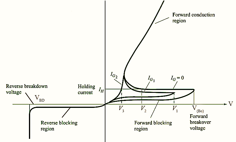
Figure 3: V-I Characteristics of Silicon Controlled Rectifier (SCR),
The voltage-current characteristics of SCR are plotted as shown in figure (3). From figure (3), it can be observed 1 that the characteristics of SCR are same as normal semiconductor diode characteristics, but in this the horizontal offshoot exist when the device is in OFF state. At IG = 0, i.e., if the voltage across gate terminal is zero, the high value of break over voltage, VBO can be observed. It indicates the device does not conduct at this point. If the voltage, VG increases at input the current, IG increases, in this case the device staffs conducting for a voltage less than VBO If the current, IG reaches certain value, the characteristics of SCR appears same as that of semiconductor diode. Further, increase in gate current, IG causes the damage to device. In forward and reverse blocking regions, the device operates in OFF state and blocks the flow of current. The avalanche breakdown occurs, when the voltage in reverse bias condition reaches breakdown voltage.
Advantages of Silicon Controlled Rectifier (SCR)
- High Efficiency: Low power loss during operation as SCR operates as a switch.
- Compact Size: Suitable for high-power applications in a small package.
- High Voltage and Current Handling: Can manage large currents and high voltages, making it ideal for industrial applications.
- Trigger Control: The gate terminal allows precise control of the switching operation.
- Durability: Rugged and reliable under proper operating conditions.
Disadvantages of Silicon Controlled Rectifier (SCR)
- Unidirectional: SCR allows current flow in only one direction, limiting its applications.
- Complex Control Circuitry: Requires additional components for gate triggering and protection.
- Switching Noise: May generate electrical noise during switching, requiring filtering.
- Latching Effect: Once turned on, it cannot be turned off via the gate; external circuits are needed for commutation.
- High Holding Current: Needs a minimum current to stay in the “on” state.
Applications of Silicon Controlled Rectifier (SCR)
- Power rectification and control in DC and AC circuits.
- Light dimmers and fan speed regulators.
- Motor control systems in industrial machinery.
- Battery charging circuits.
- Overvoltage protection systems.
- SCR can be operated as a static switch.
- It is used as zero point triggering circuit.
- These are commonly used in phase control and temperature control systems.
- In emergency lighting systems SCRs are used.
Types of Silicon Controlled Rectifier (SCR)
Silicon Controlled Rectifiers (SCRs) are classified into several types based on their construction, triggering method, and application. Below are the main types:
1. Phase-Controlled SCR
Purpose: Used in applications where the control of power is required, such as motor speed control, heater control, or dimming circuits.
Operation: The gate triggering pulse is delayed by a controlled phase angle to adjust the output power.
Examples: Light dimmers, motor drives, and voltage regulators.
2. Fast Switching SCR
Purpose: Designed for applications requiring rapid switching operations, such as high-frequency circuits.
Features: Lower turn-on and turn-off times. Smaller in size compared to standard SCRs.
Applications: Choppers, inverters, and high-speed switching circuits.
3. Light-Activated SCR (LASCR)
Purpose: Triggered using a light signal instead of an electrical gate signal.
Features: Contains a photosensitive area that responds to light. Useful in isolation and control systems where electrical signals are not preferred.
Applications: Light-triggered control systems, high-voltage AC/DC switches.
4. Reverse-Conducting SCR (RCSCR)
Purpose: Combines an SCR with a diode in reverse parallel.
Features: Used to handle both forward and reverse voltages in a single device. Reduces the need for an external diode in circuits.
Applications: Induction heating, voltage converters, and inverter circuits.
5. Bidirectional SCR (Triac)
Purpose: Can conduct current in both directions, unlike standard SCRs.
Features: Used for AC switching applications. Does not require external rectifier diodes.
Applications: AC power control, fan regulators, and light dimmers.
6. GTO (Gate Turn-Off) SCR
Purpose: Can be turned on and off by signals applied to the gate terminal.
Features: Eliminates the need for an external commutation circuit. More complex gate drive circuitry compared to standard SCRs.
Applications: Inverters, variable frequency drives (VFDs), and motor control.
7. Asymmetrical SCR (ASCR)
Purpose: Designed for applications where reverse voltage blocking capability is not required.
Features: Has a lower reverse breakdown voltage. Used in circuits where the SCR is not exposed to reverse voltage.
Applications: Phase control in rectifiers and AC/DC converters.