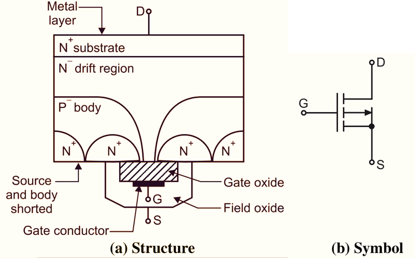
Figure 1: Power MOSFET.
A power MOSFET is a voltage controlled device and it requires a very small amount of input voltage. When we call it as a voltage controlled device, then input should be voltage. Also we always assume gate current negligible because gate is insulated. It is a high-power version of the low-power MOSFET. Relatively recent developments in technology have resulted in the production of higher- power devices with large voltage and current capabilities.
Presently, it is available with typical current rating of tens of amperes and voltage rating of hundreds of volts. It is very fast in switching speed. The switching times are of the order of nano-seconds. It does not have the problem of secondary breakdown. However, it is sensitive to electrostatic discharge and it is relatively more difficult to protect it under short-circuit condition.
Both N-channel and P-channel MOSFETs are being made, but the N-channel devices are available in higher ratings. Two types of MOSFETs are available, one called as P-channel and the other as N-channel. The P-channel devices are fabricated on N-type substrate and the N-channel devices are fabricated on P-type substrate. Two distinct types of MOSFETs are available depending on the operating modes, depletion type and enhancement type. The P-channel MOSFET works in exactly the same way as an N-channel MOSFET, only with the voltage polarities and current directions reversed.
Construction of Power MOSFET
Power MOSFET is fabricated in the form of arrays (see Figure 1(a)). This means that a single power MOSFET is in reality a parallel combination of thousands of individual cells, each being a MOSFET in itself. The number of cells on a silicon pellet may be as high as 1000 on an area as small as 1mm2. The MOSFET has three external terminals called Drain D, Source S and Gate G. The drain and source are the power terminals of the switch. The gate is the control terminal. The control voltage to implement turn-ON is applied between the gate and the source terminals. The direction of the forward current flow in an N-channel MOSFET is from the drain to the source. This results in the flow of electrons from the source to the drain. Fig. 1 (a) shows the junction structure of a depletion type N-channel power MOSFETs. The N-layer on the top constitutes the drain. This layer is actually made up of an outer N+ layer of low resistivity, i.e. higher concentration of carriers and an inner N+ layer of high resistivity, i.e. low impurity concentration. The inner high sensitivity region serves to give a high voltage capability, while the outer low resistivity region serves to make a strong low resistance electrical contact with the drain surface metal deposition. Adjacent to the N+ region, there is a relatively large P isolated as shown in Fig. 2.40 (a). Inside the P islands and also the middle part of the P island between the N+ islands. The gate terminal does not make any electrical contact with the silicon pellet because of the presence of layer of silicon dioxide (SiO2) which is an insulator between the surface and the gate. The gate zone is over the P island between the N+ drain region and the N+ source region. A conditioning polycrystalline silicon layer, deposited over the gate zone, on the silicon dioxide layer serves as the gate layer. The polycrystalline silicon layer gives better performance than the deposited metal layer. Fig. 1 (b) shows the symbol of an N-channel depletion type power MOSFET.
Working Principle of Power MOSFET
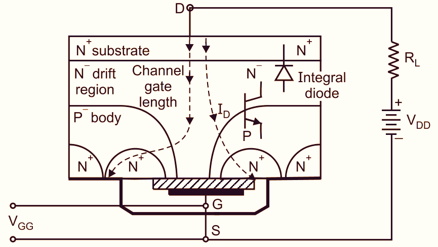
Figure 2: Operation of N-channel power MOSFET
Consider the circuit of N-channel power MOSFET as shown in Fig. 2. The drain terminal D is made positive with respect to the emitter terminal E so that it is reverse biased. Now the gate is kept open i.e. VGE = 0. Under this situation, the junction N– P– is reverse biased and hence no drain current ID flows from drain-to-source. Only very low reverse leakage current can flow through it. Thus the power MOSFET does not conduct. This is a forward blocking (OFF) state of a power MOSET. When a low positive gate voltage VGS is applied at the gate G, it creates the electric field which pulls the electrons from the N+ region into the P region immediately near the gate G. This forms an N-channel. Thus the source N+ region gets linked with the drain N+ region and the N-channel provides the path for flow of current. So, the drain current ID flows from drain to source depending upon the voltage level VDD. As then the drain voltage VDS is increased further, the drain current ID increases and then remains constant. This is the forward conduction (ON) state of a power MOSFET. This conduction is due to the majority charge carriers alone. Hence the time delay caused by removed or recombination with minority carriers is eliminated and so power MOSFET can switch ON only at frequencies in MHz range.
Characteristics of Power MOSFETs
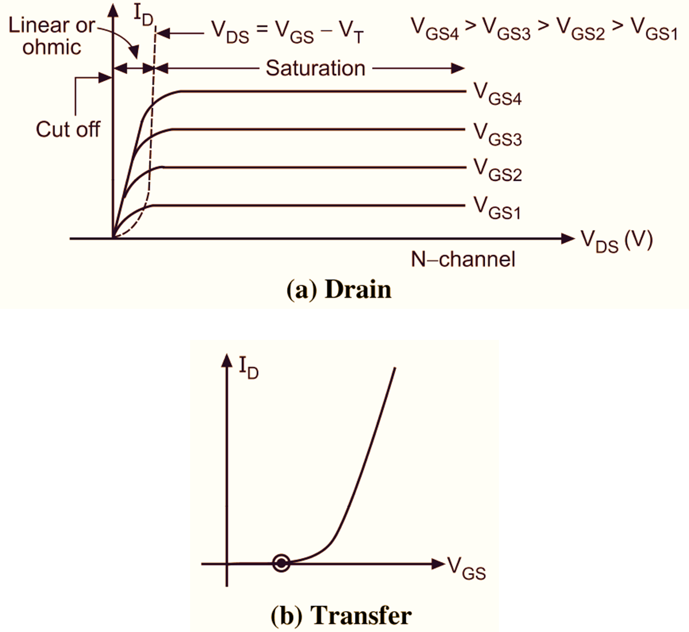
Figure 3: Drain and transfer characteristics of N-channel power MOSFET
1. V-I characteristics :
These characteristics are plotted as the variation in drain current (ID) as a function of drain source voltage (VDS) for a given value of (VGS). For low values of VDS, the characteristics are linear and the device exhibits a constant ON-state resistance. If VDS is increased further, then the drain current saturates. This is shown in Fig. 3 (a). Three regions are shown above in the output characteristics as :
- Ohmic or linear : The output current ID varies linearly with VDS.
- Saturation : The current ID saturates if VDS is increased further.
- Cut-off : The current ID is zero because VGS is zero and no N channel is formed.
2. Transfer characteristics :
The characteristics of drain current (ID) against gate-source voltage (VGS) are called transfer characteristics. The threshold voltage (VT) is that value of VGS at which N-channel is formed and the drain current starts flowing. The transfer characteristics of N channel power MOSFET are shown in Fig. 3 (b).
Advantages of Power MOSFETs
The important advantages of power MOSFETs are as given below :
- It has fast switching speed.
- It has extremely low drain resistance rDS(on).
- It has very high input impedance of about 109 Ω.
- It is very simple for construction.
- It is free from secondary breakdown.
- It has ease of paralleling.
- It has excellent temperature stability.
- It has very high operating frequency.
- The switching times are essentially independent of temperature.
- It has very high current gain of the order of 109.
The switching times (turn-ON and turn-OFF) are very low around 30 to 40 ns for a 40 V, 50 A power MOSFET and around 190 ns for a 500 V, 25 A power MOSET. Due to this low turn-OFF time, the power MOSFET can be operated at a frequency of I MHz to 10 MHz.
Applications of Power MOSFET ;
The important applications of power MOSFET are as given below :
- It is widely used in analog and digital signal processing circuits both in discrete and integrated circuit (IC) forms.
- It can be used as a static switch or for analog operation.
- It can be used in SMPS, solid state d.c. relay, brushless d.c. motor drives and automobile applications.
Features of Power MOSFET
MOSFETs are preferred over power BJTs in applications requiring high switching speeds. MOSFETs may be of P-channel type or N-channel type depending on whether the channel material is of P-type or N-type. Further MOSFET be either enhancement type or depletion type.
Difference between BJT and MOSFET
| MOSFET | BJT |
| It is a unipolar device. | It is a bipolar device. |
| It produces less noise. | More noise than MOSFET. |
| It is voltage controlled. | It is current controlled. |
| Input impedance is higher. | Input impedance is lower than MOSFET. |
| Better thermal stability. | Less thermal stability. |
| Relatively less affected by radiation. | More impact due to radiation. |
| It is compact and easy to fabricate in integrate circuits. | It is not as easy and compact as MOSFET. |
| It is free from secondary breakdown. | Secondary breakdown occurs. |