The voltage gain of the Voltage Follower (Buffer) circuit is 1 i.e. the output voltage will be equal to and in phase with the input voltage. In other words, the output voltage follows the input voltage. Hence the name voltage follower. Thus voltage follower is a non-inverting amplifier with a voltage gain of unity.
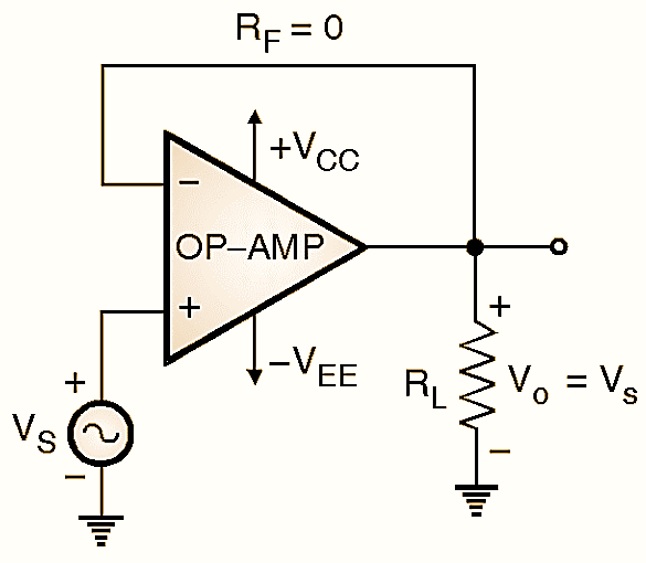
Figure 1: Voltage Follower (Buffer) Circuit Diagram.
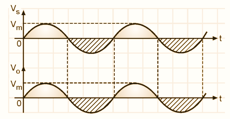
Figure 2: Waveforms of Voltage Follower (Buffer).
Circuit diagram of Voltage Follower (Buffer) Using Op-Amp
When R1 = ∞ and RF = 0 the non-inverting amplifier gets converted into a voltage follower or unity gain amplifier. When the non-inverting amplifier is configured so as to obtain a gain of 1, it is called as a voltage follower or unity gain non-inverting buffer. The schematic diagram for a voltage follower is as shown in Fig. 1. The voltage follower configuration of Fig. 1 is obtained by short circuiting RF and open circuiting R1 connected in the usual non-inverting amplifier configuration of Fig. 1. Thus all the output voltage is fed back to the inverting input of the OP-AMP. Therefore the feedback factor of this circuit i.e. B = 1.
Closed Loop Voltage Gain (AVF) of Voltage Follower (Buffer) Using Op-Amp
Consider the expression for the closed loop gain of a non-inverting amplifier, that is,
\[{{A}_{VF}}=1+\frac{{{R}_{F}}}{{{R}_{1}}}….(1)\]
In above equation 1, substitute the values of RF = 0 and R1 = ∞ to get the closed loop gain of the voltage follower as,
\[{{A}_{VF}}=1\]
Therefore the output voltage will be equal to and in phase with the input voltage, as shown in Fig. 2. Thus voltage follower is a non-inverting amplifier with a voltage gain of unity.
Why Voltage Follower is called a buffer?
A buffer is an electronic circuit that isolates the input from the output, providing either no voltage or a voltage that is the same as the input voltage. It has a voltage gain of unity (1). A voltage buffer must have a very high input impedance and very low output impedance so that it draws a very small current from input and can supply. Since a voltage follower circuit satisfies all these requirements, it is called as a buffer.
Applications of Voltage Follower (Buffer) Using Op-Amp
- As a buffer amplifier so as to avoid the loading of the source.
- It is used as the output stage because of its low Ro.
- It can be used for impedance matching.