Charge Coupled Device (CCD) is a simple shift register used to store and transfer analog signals and electrically or optically injected charge carriers.
Construction of Charge Coupled Device
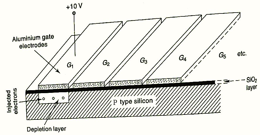
Figure 2: Charge Coupled Device Structure.
The structure of a three-phase charge-coupled device is as shown in figure (1). The basic structure of CCD comprises of series of metal gate electrodes that are connected to an external supply and a P-type semiconductor silicon substrate or N-type substrate which are separated by a thin layer of silicon dioxide.
Working of Charge Coupled Device
A three-phase clocked voltage pulse system provides supply to gate electrodes. The charge is serially coupled between the electrodes, the charge transformation process in CCD is explained.
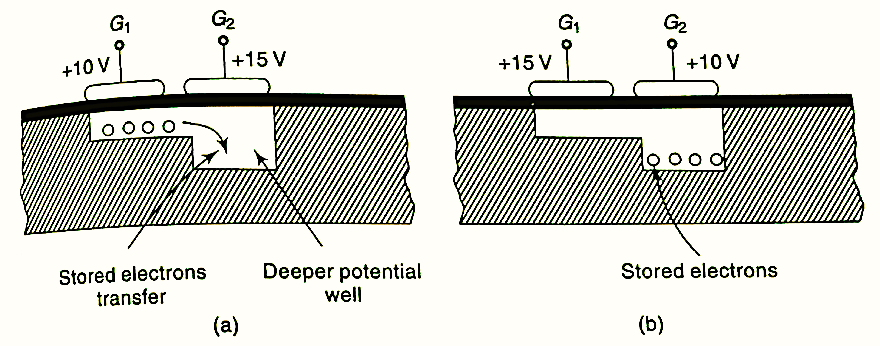
In the first phase, the signal voltage V1 = 10 V is applied to gate G1. Due to the motion of charge carriers, a thin layer of depletion region is developed, which further creates a potential well. The information is stored in potential well in the form of minority electrons.
In the second phase, the signal voltage V2 = + 15 V is applied to gate, G2. It forms a potential well deeper than that is created by G1. The stored electrons than moved into the well under G2 and the voltage at terminal G1 and G2 becomes + 5 V and + 10 V respectively. The electrons from one well to another well are transferred easily when there is an overlap between them. This can be attained by maintaining sufficient space between adjacent gates.
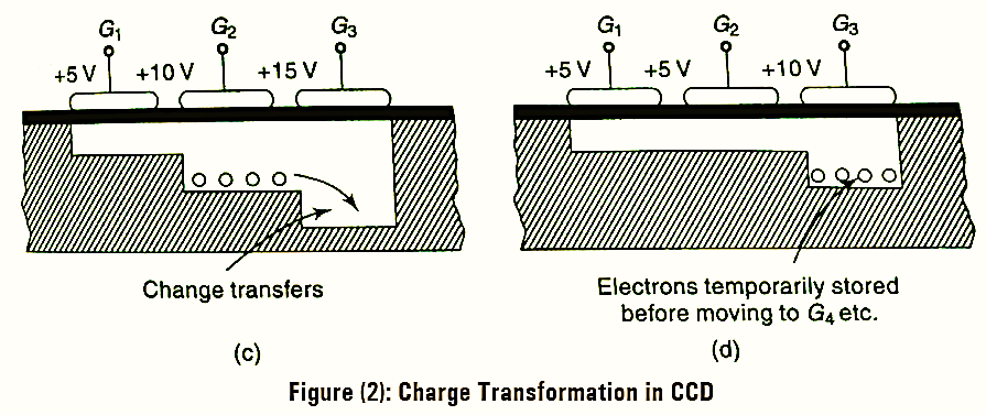
Similarly in third phase, the gate G3 is provided with a supply of + 15V. This creates a potential well deeper than that under G2, so the charge carriers then transfer into the well under G3. The voltages at gate electrodes G1, G2 and G3 become + 5V, + 5V and + IOV respectively. The diagrammatic representation of charge coupling in CCD is illustrated in figure (2).
The transfer of charge from electrodes G1 to G3 requires a one-clock period or frequency and in this duration, only single-bit information is transmitted from one electrode to another.
The information is provided again at the input gate for every one clock period. This is a repetitive process and can be observed between every three neighboring electrodes.
This process is valid only when the charge leaves a specific well in a time less than 1 ms. Otherwise, an inversion layer is formed and charge carriers disappear so that the respective bit information is lost within the device.
Advantages of Charge Coupled Device
The advantages of CCDs are mentioned as follows,
- The packing density of CCDs is more than that of semiconductor devices.
- The power consumption in CCDs is less.
Applications of Charge Coupled Device
The applications of CCDs are given as follows,
- In memory devices
- Imaging field and a solid state color TV camera.
- These are used in photo sensors.
- Analog signal applications such as transversal filters, recursive filters, pulse compressors and pulse expanders.
- In computers and video cameras.