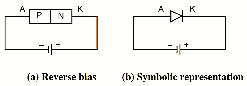
When the anode terminal of a diode is connected to the negative terminal of voltage source and cathode to the positive terminal then the diode is reverse biased as shown in Fig. 1 (a) and its symbolic representation in Fig. 1 (b).
Operation of Reverse Biased PN Junction Diode
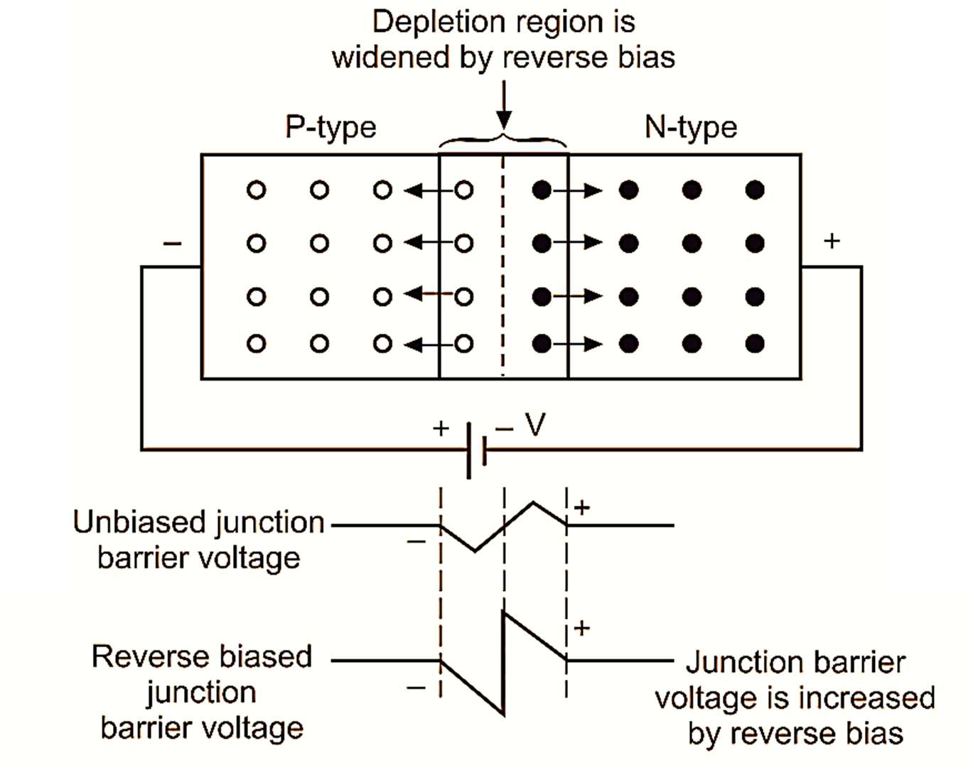
Figure 2: Reverse biased effect on layer and barrier voltage.
When an external bias is applied to a diode, positive to cathode and negative to anode, electrons from N-side are attracted to the positive terminal and holes from P-side are attracted to the negative terminal. As shown in Fig. 2, holes on P-side of junction are moved away from the junction and electrons are also moved away from the junction on N-side. This results in the depletion region to be widened and the barrier voltage to be increased.
As the barrier voltage at the junction increases, the holes and electrons are not able to cross the junction, hence the majority charge carrier current will be zero and the junction is said to be reverse biased. There will be very small reverse current due to minority charge carrier. Because of this very small reverse current flow, a reverse biased PN junction diode offers very high resistance. As there is no possibility of majority charge carriers the current flowing across a reverse biased junction, minority carriers i.e. holes on N-side and electrons on P-side, generated on each side can cross the reverse junction. The electrons on the P-side are attracted to the positive voltage crossing the junction on the N-side. The holes from N-side flow across to the negative voltage on P-side. Due to this, small current flows through the junction. Only a very small reverse bias voltage is necessary to move all available minority carriers across the junction and if voltage bias is increased further, current will not increase. And hence this current is referred as reverse saturation current. The reverse saturation current is very small ranging from nanoamperes to microamperes. It depends on the junction area, temperature and semiconductor material.