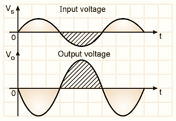
In Inverting Amplifier, the amplified output signal will be 180º out of phase with the input signal. In other words the output signal is “inverted” as shown in Fig. 2. Therefore this amplifier is known as the inverting amplifier.

Figure 1: Inverting Amplifier.
Circuit diagram of Inverting Amplifier Using Op-Amp
The circuit diagram of an inverting amplifier is as shown in Fig. 1. The signal which is to be amplified is applied at the inverting (-) input terminal of the OP-AMP.
Working and Waveforms of Inverting Amplifier Using Op-Amp
The signal to be amplified (Vs) has been connected to the inverting terminal via the resistance R1. The other resistor RF, connected between the output and inverting input terminals is called as the feedback resistance. It introduces a negative feedback. The non-inverting (+) input terminal is connected to ground. As the OP-AMP is an ideal one, its open loop voltage gain Av = ∞ and input resistance Ri = ∞. The negative sign for Av is due to the inverting configuration. The input and output voltage waveforms are as shown in Fig. 2. Output is an amplified and inverted version of the input signal VS.
Closed Loop Voltage Gain (AVF) of Inverting Amplifier Using Op-Amp
Looking at Fig. 1 we can write that,
\[{{V}_{o}}=\left| {{A}_{v}} \right|\times {{V}_{d}}\]
\[{{V}_{d}}=\frac{{{V}_{o}}}{\left| {{A}_{v}} \right|}\]
Where,
Av = Open loop gain of OP-AMP.
As we know an open loop gain of OP-AMP is ∞.
\[{{V}_{d}}=\frac{{{V}_{o}}}{\infty }=0\]
But,
\[{{V}_{d}}={{V}_{1}}-{{V}_{2}}\]
\[{{V}_{1}}-{{V}_{2}}=0….(1)\]
As the non-inverting (+) input terminal is connected to ground, V1 = 0. Substituting this value in Equation (1) we get,
\[{{V}_{2}}=0\]
Thus V2 is at ground potential. Since the input resistance Ri = ∞, the current going into the OP-AMP will be zero. Therefore the current “I” that passes through R1 will also pass through RF as shown in Fig. 1. As the input voltage VS is being measured with respect to ground and as V2 is at ground potential we can say that the input voltage V2 is voltage across R1 and voltage across RF is output voltage. The input voltage, VS is given by,
\[{{V}_{S}}=I\text{ }{{R}_{1}}….(2)\]
And the output voltage Vo is given by,
\[{{V}_{o}}=-I\text{ }{{R}_{F}}….(3)\]
We can write Equations (2) and (3) because V2 is at approximately ground potential (virtual ground).
\[\text{Closed loop gain, }{{A}_{VF}}=\frac{{{V}_{o}}}{{{V}_{S}}}\]
Substituting the expression for Vo and VS we get,
\[{{A}_{VF}}=-\frac{I{{R}_{F}}}{I{{R}_{1}}}=-\frac{{{R}_{F}}}{{{R}_{1}}}….(4)\]
And,
\[{{V}_{o}}={{A}_{VF}}\times {{V}_{S}}\]
Conclusions from the expression for AVF :
From Equation (4) we can draw the following important conclusions :
- The value of closed loop voltage gain AVF does not depend on the value of open loop voltage gain Av.
- Value of AVF can be very easily adjusted by adjusting the values of the resistors RF and Ri. Generally the feedback resistor RF is a potentiometer to adjust the gain to its desired value.
- The output is an amplified inverted version of input.