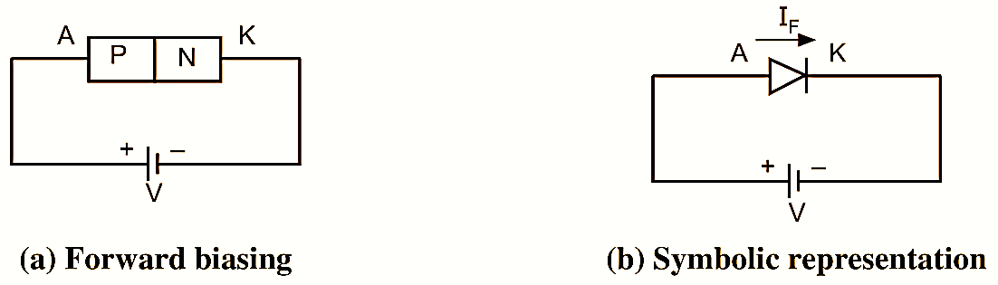
Figure 1.
When anode is connected to the positive terminal of a battery/voltage source and cathode to the negative terminal, then the diode is said to be forward biased as shown in Fig. 1 (a) and its symbolic representation is shown in Fig. 1 (b).
Operation of Forward Biased PN Junction Diode
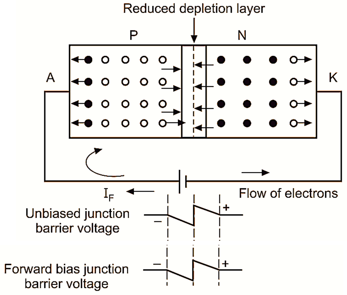
Figure 2: Forward biased effect on layer and barrier voltage.
When PN junction is forward biased, the holes (being positively charged) are repelled by the positive terminal of voltage source and forced to move towards the junction. Similarly, the electrons (negatively charged) are repelled by the negative terminal of voltage source and move towards the junction. As they get some energy from the voltage source, some of the holes and electrons enter the depletion layer and recombine themselves. This results in reduction in width of depletion layer and the barrier potential with forward bias as shown in Fig. 2. Therefore, it causes a large current to flow through the diode. When the applied bias voltage is increased from zero, the barrier voltage gets decrease until it effectively disappears and majority charge carriers easily flow across the junction. The electrons from N-side are now attracted across to the positive bias terminal on P-side and holes from the P-side flow across to the negative terminal on the N-side. Thus, a majority carrier current flows and the junction is said to be forward biased. This large current due to majority charged carrier in forward biased is called as forward current.